
The Hidden Water Cost of Your Devices
Water doesn’t usually feature in conversations about electronics sustainability. Carbon emissions, rare minerals, and landfill waste dominate the narrative. But the water footprint of electronics manufacturing is staggering, and it’s a dimension of environmental impact that deserves far more attention than it currently receives, particularly in a water-stressed country like Australia.
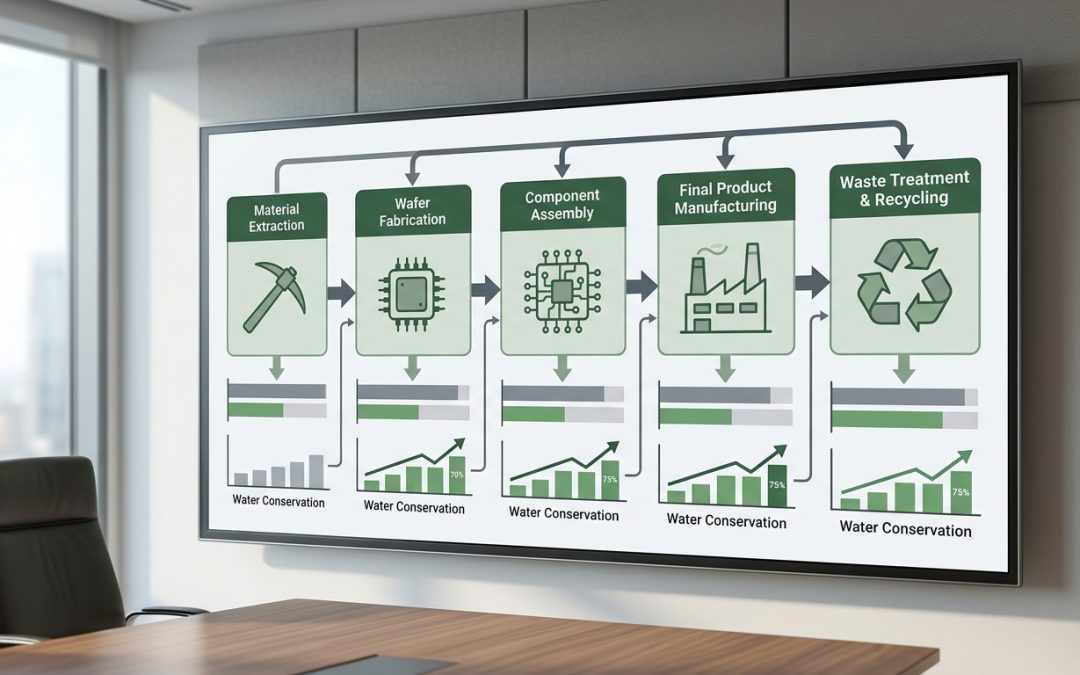
Every electronic device you own required enormous quantities of water to produce. From mining the raw materials to fabricating semiconductor chips to assembling the final product, water is consumed, contaminated, and discharged at every stage. Understanding this hidden water cost adds an important dimension to the environmental case for extending device lifespans and recycling electronics responsibly.
The Numbers
The water intensity of electronics manufacturing is driven primarily by semiconductor fabrication. Modern chip manufacturing requires ultra-pure water (UPW) for cleaning wafers between processing steps, and the quantities involved are enormous. A single semiconductor fabrication facility (fab) can consume 30-50 million litres of water per day, roughly equivalent to the daily water use of a city of 50,000-100,000 people.
Translating this to individual devices: manufacturing a single semiconductor chip requires approximately 30-35 litres of ultra-pure water. A smartphone, which contains multiple chips along with other water-intensive components, carries a total water footprint estimated at 12,000-13,000 litres when all manufacturing stages are included. A laptop’s water footprint is roughly 40,000-50,000 litres.
To put these numbers in context: the water footprint of manufacturing a single smartphone is equivalent to roughly 80 bathtubs of water. For a laptop, it’s closer to 300 bathtubs. These figures include direct water use in manufacturing, water used in electricity generation that powers manufacturing, and water consumed in mining and processing raw materials.
Smartphone: ~12,000-13,000 litres
Laptop: ~40,000-50,000 litres
Desktop computer: ~50,000-70,000 litres
Server: ~100,000+ litres
For reference, the average Australian uses approximately 200 litres of water per day for all household purposes.
Where the Water Goes
Mining and material processing accounts for a significant portion of electronics’ water footprint. Mining copper, gold, lithium, and other minerals requires water for extraction, crushing, grinding, and chemical separation processes. Many mining operations are located in arid regions, creating competition with local water needs. The tailings (waste material) from mining operations can contaminate water sources if not properly managed.
Semiconductor fabrication is the most water-intensive manufacturing step. Each silicon wafer goes through hundreds of processing steps, many of which involve washing with ultra-pure water to remove contaminants that would ruin the nanoscale circuits. The water must be purified to extraordinary standards, far purer than drinking water, which itself requires significant energy and produces waste concentrate streams.
Printed circuit board manufacturing uses water in etching processes, plating baths, and cleaning operations. The chemical-laden wastewater from PCB manufacturing requires careful treatment before discharge, and improper handling has been a source of water pollution in manufacturing regions.
Display manufacturing involves water-intensive cleaning and processing steps, particularly for the glass substrates and thin-film deposition processes used in LCD and OLED panels.
The Geographic Dimension
The environmental significance of water use depends heavily on where the water is consumed. Using 50,000 litres of water in a region with abundant fresh water supplies has different ecological consequences than using the same amount in a water-stressed region. This concept, known as water stress weighting, is increasingly incorporated into environmental impact assessments.
Unfortunately, much of the world’s electronics manufacturing is concentrated in regions facing significant water stress. Taiwan, home to the world’s largest semiconductor manufacturer (TSMC), experiences periodic droughts that have forced water rationing and affected chip production. Parts of China, South Korea, India, and the southwestern United States where electronics manufacturing is concentrated also face growing water stress due to climate change and competing demands from agriculture, industry, and growing urban populations.
Australia’s position as a technology consumer rather than manufacturer means that the water footprint of electronics used here is largely embedded in imported products. This is sometimes called a “virtual water import,” and it means that Australian electronics consumption contributes to water stress in manufacturing regions even though the physical water use occurs overseas.
Water Contamination Concerns
Beyond consumption, electronics manufacturing poses significant water contamination risks. The chemicals used in semiconductor fabrication, PCB manufacturing, and surface treatment processes include solvents, acids, heavy metals, and per- and polyfluoroalkyl substances (PFAS). If wastewater treatment systems fail or are inadequate, these substances contaminate local water supplies.
PFAS contamination from electronics manufacturing has become a particular concern globally. These “forever chemicals” are used in various manufacturing processes and don’t break down in the environment. Contamination of groundwater near semiconductor fabs and electronics manufacturing facilities has been documented in multiple countries.
Improper e-waste processing also contributes to water contamination. When electronic waste is processed informally, such as through acid leaching of circuit boards or open-air burning, heavy metals and toxic chemicals enter soil and water systems. This connects the e-waste export problem discussed in the context of circular economy goals directly to water quality impacts in receiving communities.
Why This Matters for Device Lifespans
The water footprint adds another powerful argument for extending electronics lifespans. Every device that’s replaced prematurely triggers the manufacturing of a new device, with its full water footprint. By keeping devices in productive use longer through maintenance, repair, and refurbishment, the annualised water consumption per year of computing service decreases dramatically.
A laptop used for three years consumes approximately 15,000 litres of embedded water per year of use. The same laptop used for six years halves that to approximately 7,500 litres per year. Extending to nine years (through refurbishment and redeployment) reduces it to roughly 5,000 litres per year. The same logic applies to recycling recovered materials back into manufacturing, which uses a fraction of the water required for processing virgin materials.
For organisations tracking their environmental footprint, water consumption in supply chains (often categorised under Scope 3 impacts) is gaining prominence alongside carbon emissions. Understanding the water dimensions of IT procurement and disposal decisions supports more comprehensive sustainability reporting and more informed environmental strategy.
The water footprint of electronics is enormous, largely invisible, and concentrated in regions that can least afford to bear it. Making this hidden cost visible is an important step toward more sustainable electronics consumption.
EWV helps Victorian businesses manage e-waste and IT asset disposal compliantly and sustainably — including collection, certified data destruction, and recycling. Contact us for a free quote.